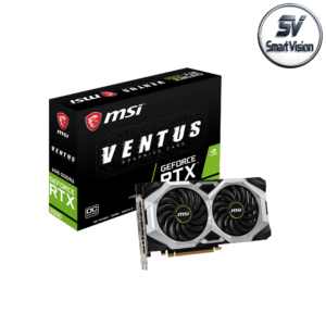
GeForce GTX 950 2G AMP! Editio...
3,000 EGP
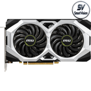
Gigabyte GTX 1060 6G GAMING G1
6,000 EGP

GeForce GTX 750 1GB
Brand:
29 people are viewing this product right now
1,500 EGP
Estimated delivery:20 July، 2026
Categories: Used Graphic Card
Share this product:
Have any Questions?
Feel free to Get in touch.
Graphics Processor
GPU Name
GM107
GPU Variant
GM107-300-A2
Architecture
Maxwell
Foundry
TSMC
Process Size
28 nm
Transistors
1,870 million
Density
12.6M / mm²
Die Size
148 mm²
Chip Package
FCBGA-908
Graphics Card
Release Date
Feb 18th, 2014
Generation
GeForce 700
Predecessor
GeForce 600
Successor
GeForce 900
Production
End-of-life
Driver Support
Active
Launch Price
119 USD
Bus Interface
PCIe 3.0 x16
Reviews
10 in our database
Clock Speeds
- Base Clock
- 1020 MHz
- Boost Clock
- 1085 MHz
- Memory Clock
- 1253 MHz
5 Gbps effective
Memory
- Memory Size
- 1024 MB
- Memory Type
- GDDR5
- Memory Bus
- 128 bit
- Bandwidth
- 80.19 GB/s
Render Config
- Shading Units
- 512
- TMUs
- 32
- ROPs
- 16
- SMM Count
- 4
- L1 Cache
- 64 KB (per SMM)
- L2 Cache
- 2 MB
Theoretical Performance
- Pixel Rate
- 17.36 GPixel/s
- Texture Rate
- 34.72 GTexel/s
- FP32 (float)
- 1,111.0 GFLOPS
- FP64 (double)
- 34.72 GFLOPS (1:32)
Board Design
- Slot Width
- Single-slot
- Length
- 145 mm
5.7 inches
- TDP
- 55 W
- Suggested PSU
- 250 W
- Outputs
- 2x DVI
1x mini-HDMI 1.4a
- Power Connectors
- None
- Board Number
- P2010 SKU 51
Graphics Features
- DirectX
- 12 (11_0)
- OpenGL
- 4.6
- OpenCL
- 3.0
- Vulkan
- 1.4
- CUDA
- 5.0
- Shader Model
- 6.7 (5.1)
Only logged in customers who have purchased this product may leave a review.
Related products
1 in stock
Out of stock
1 in stock
Out of stock
Out of stock
Reviews
There are no reviews yet.